

 Deposition
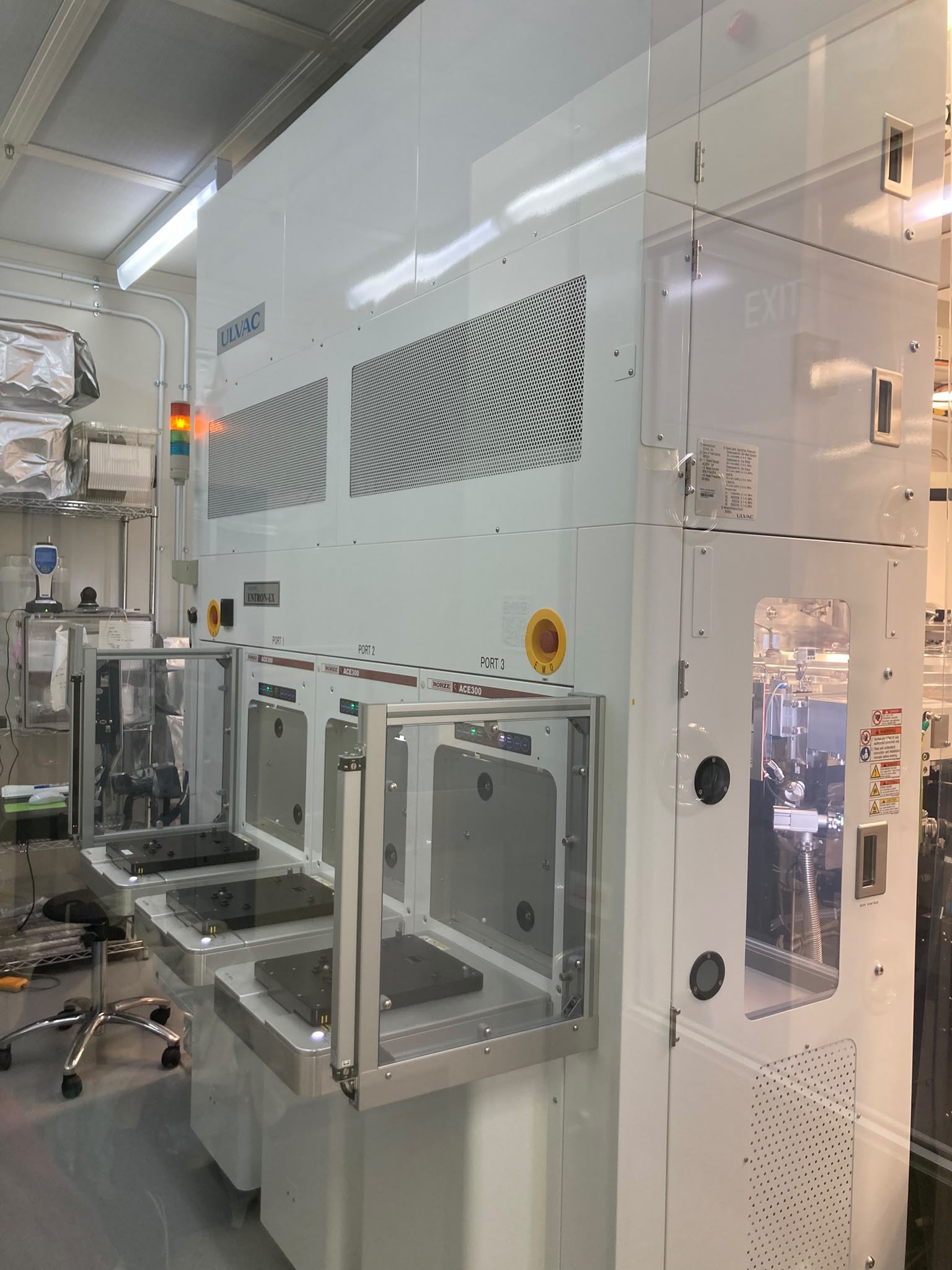
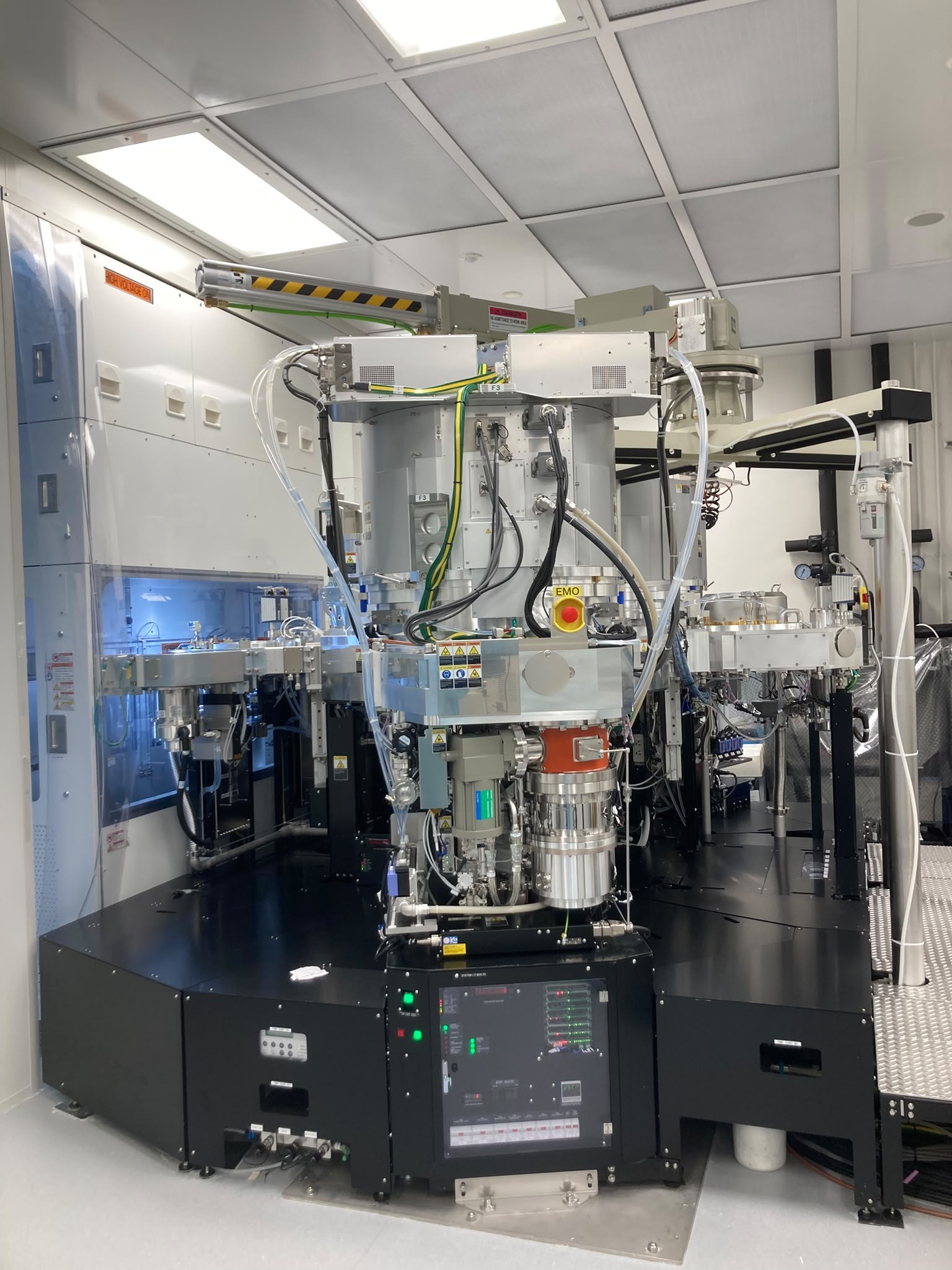
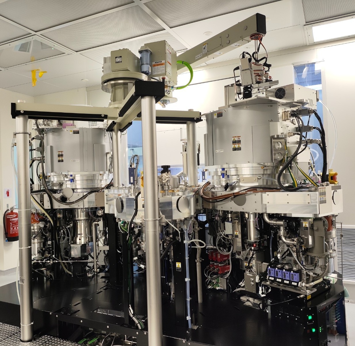
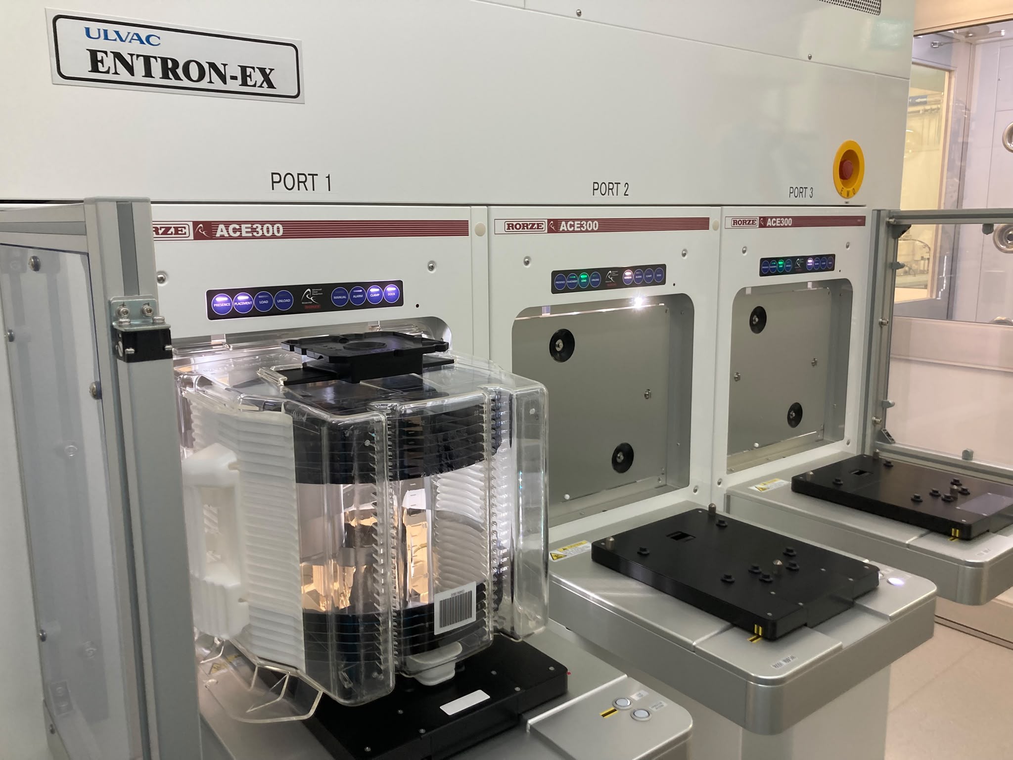
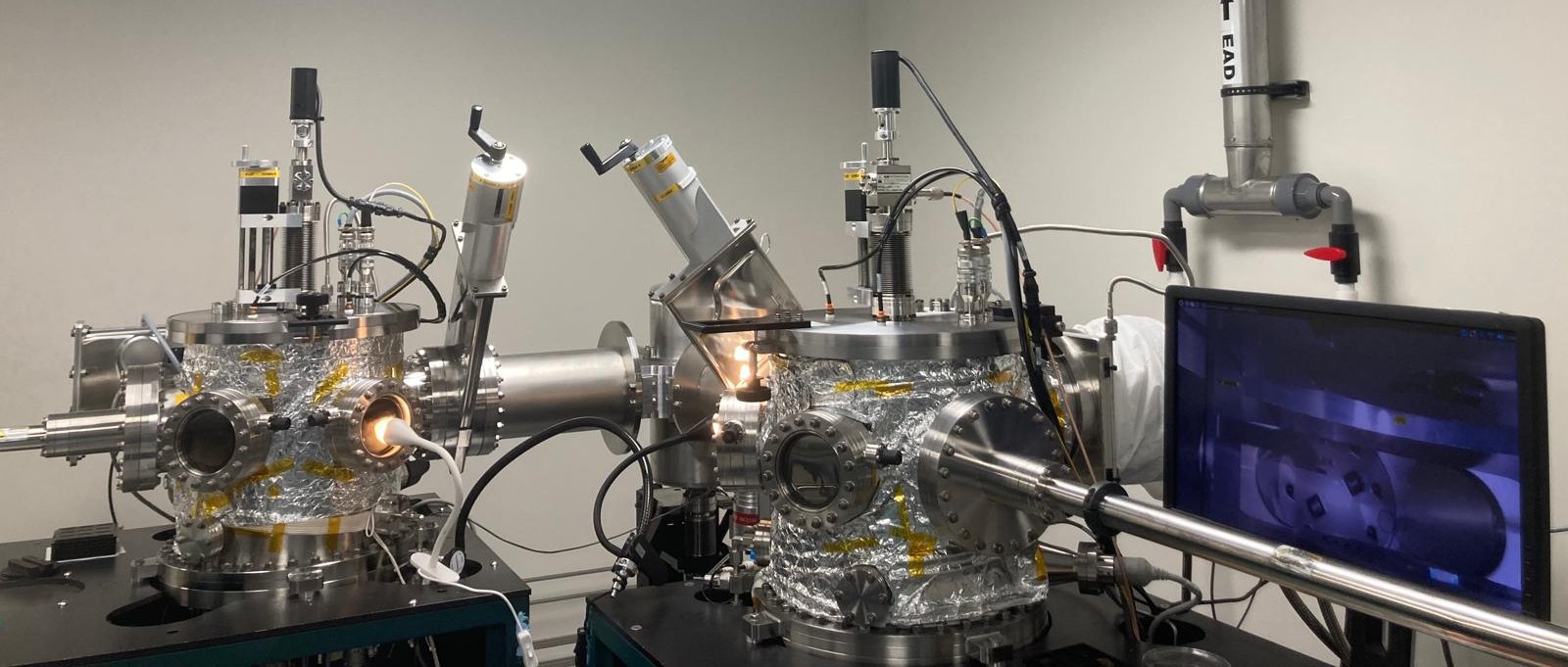
ULVAC ENTRON-EX 300 mm PVD System
An industry-grade, high-performance, multi-chamber sputtering deposition system featuring automated robotic wafer handling and integrated hydrogen plasma treatment capabilities. The system enables high-precision thin-film deposition with excellent process control, making it ideal for fabricating non-volatile memory stacks and advanced semiconductor device structures.
 Deposition
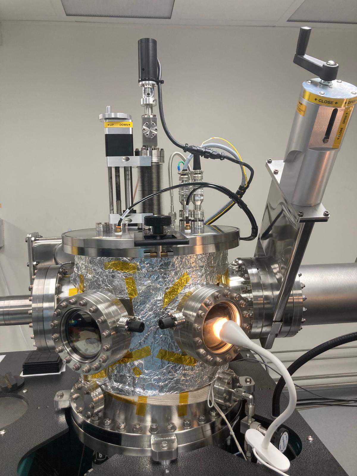
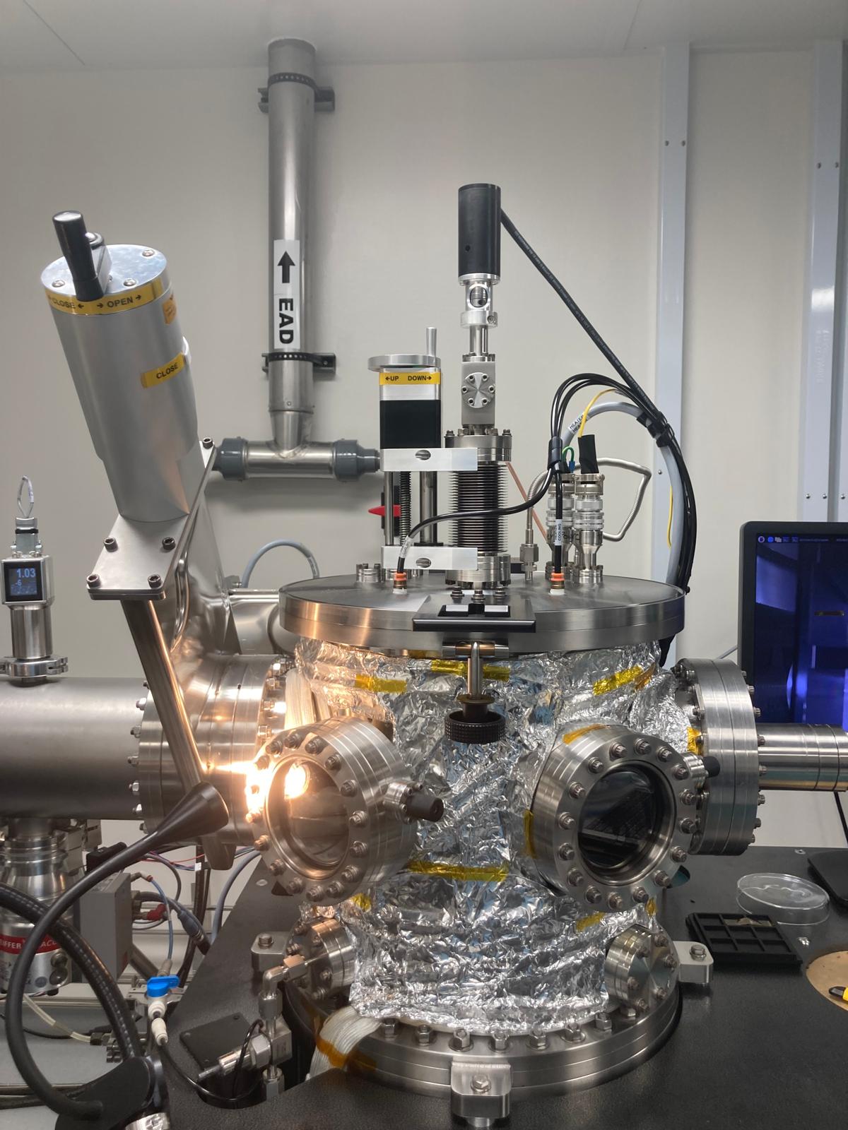
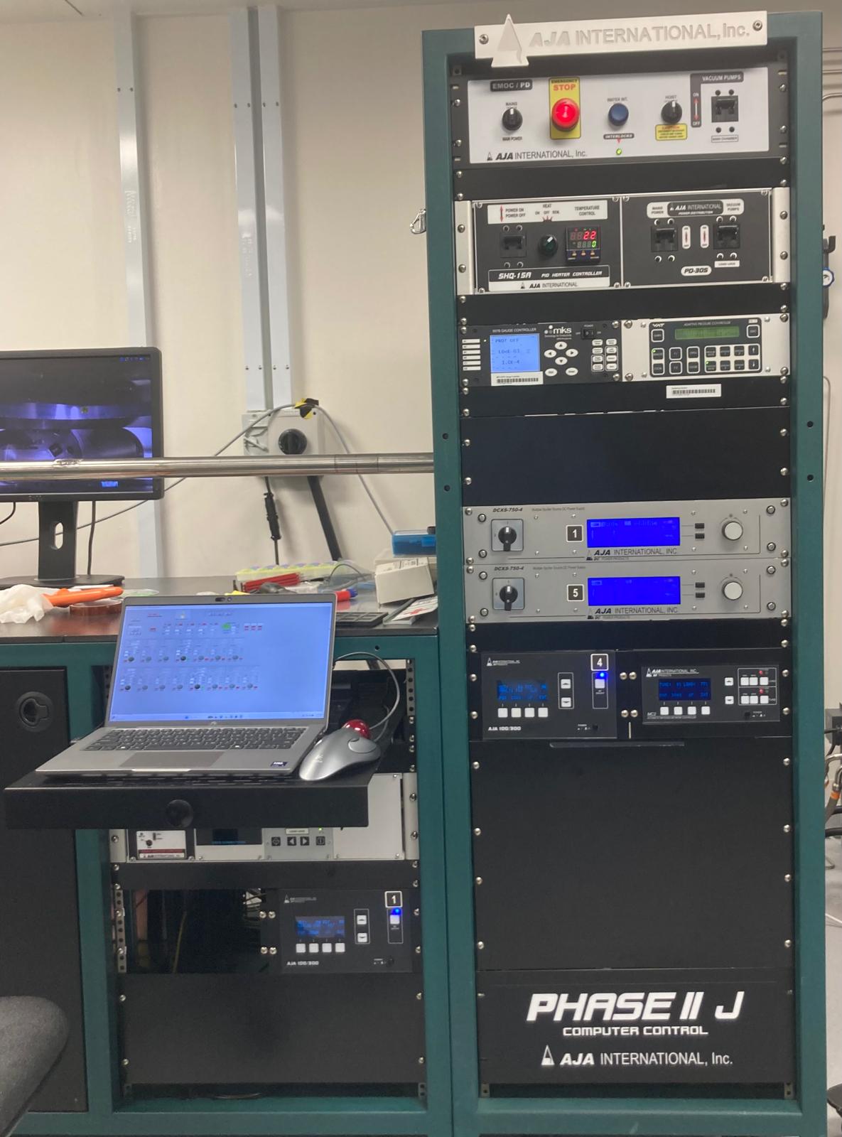
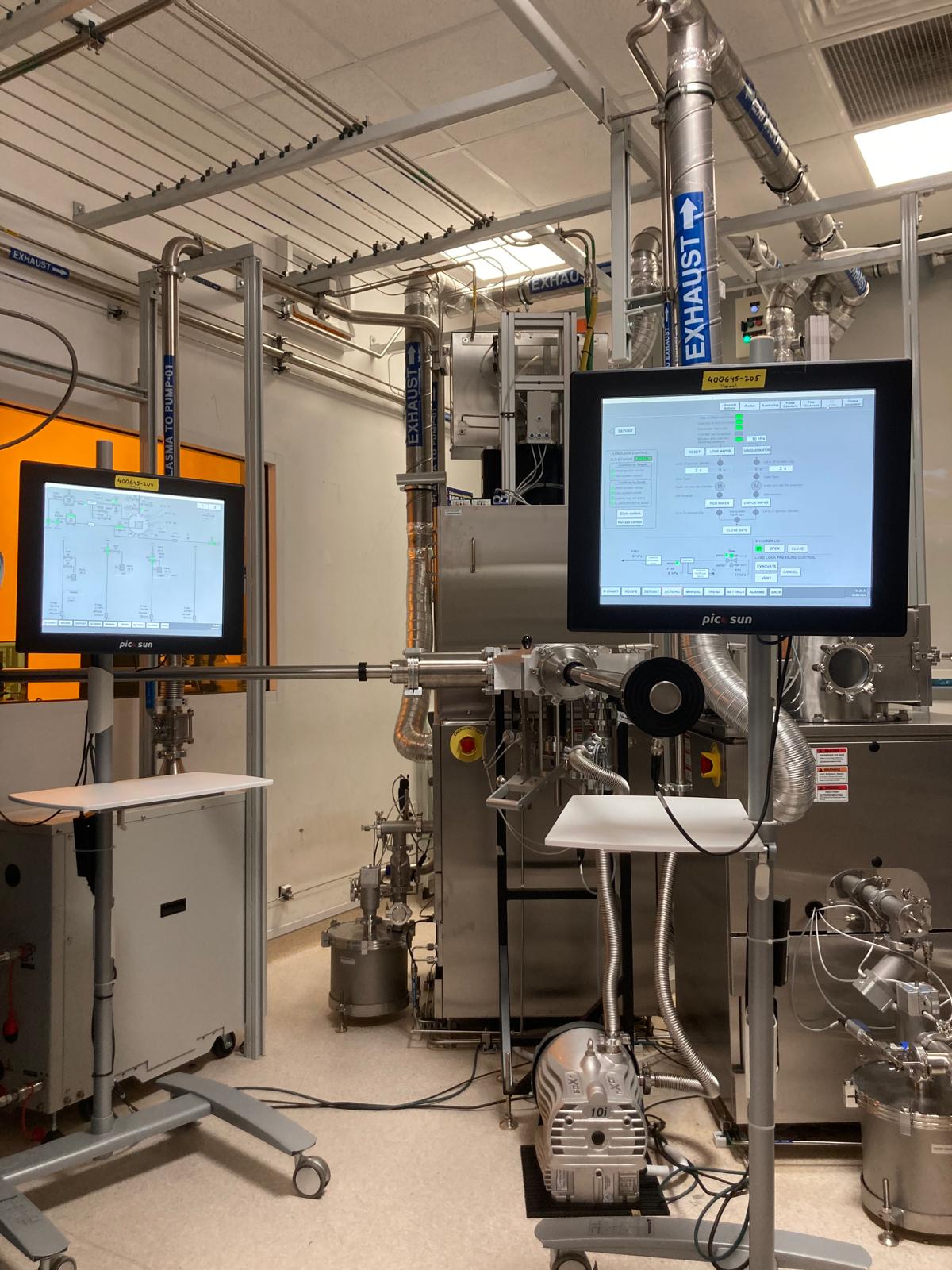
AJA 16–Target Dual-Chamber UHV Magnetron Sputtering System
Two interconnected 8-target ultrahigh vacuum magnetron sputtering systems, enabling the growth of MRAM, ReRAM and FeRAM thin film stacks.
 Deposition
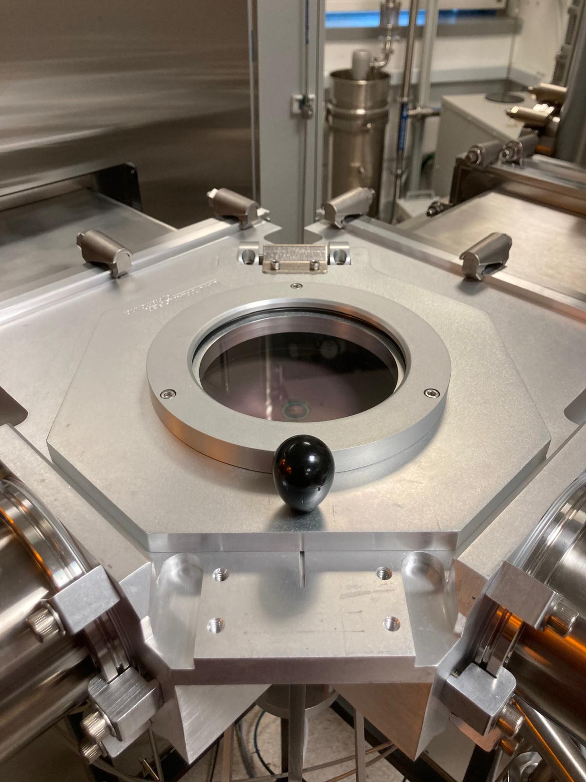
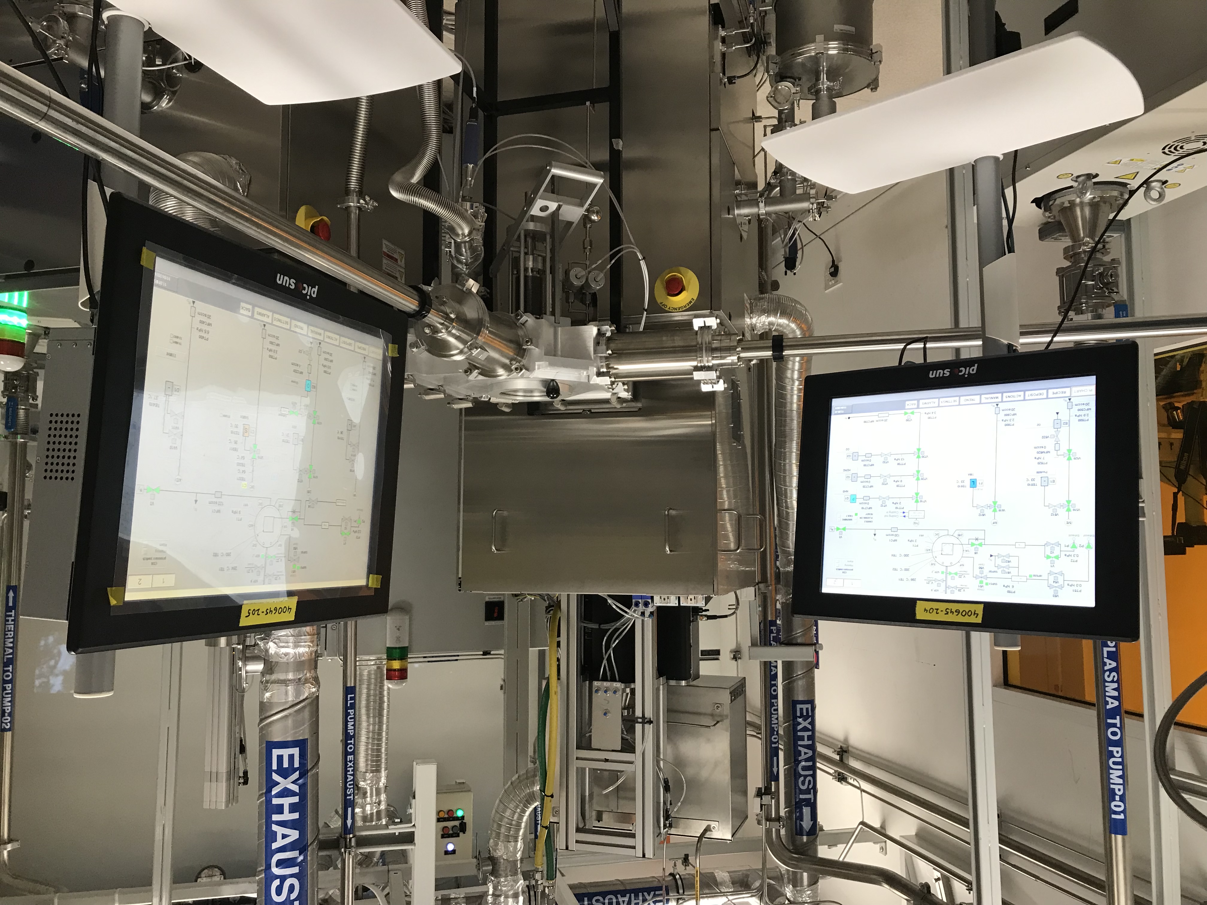
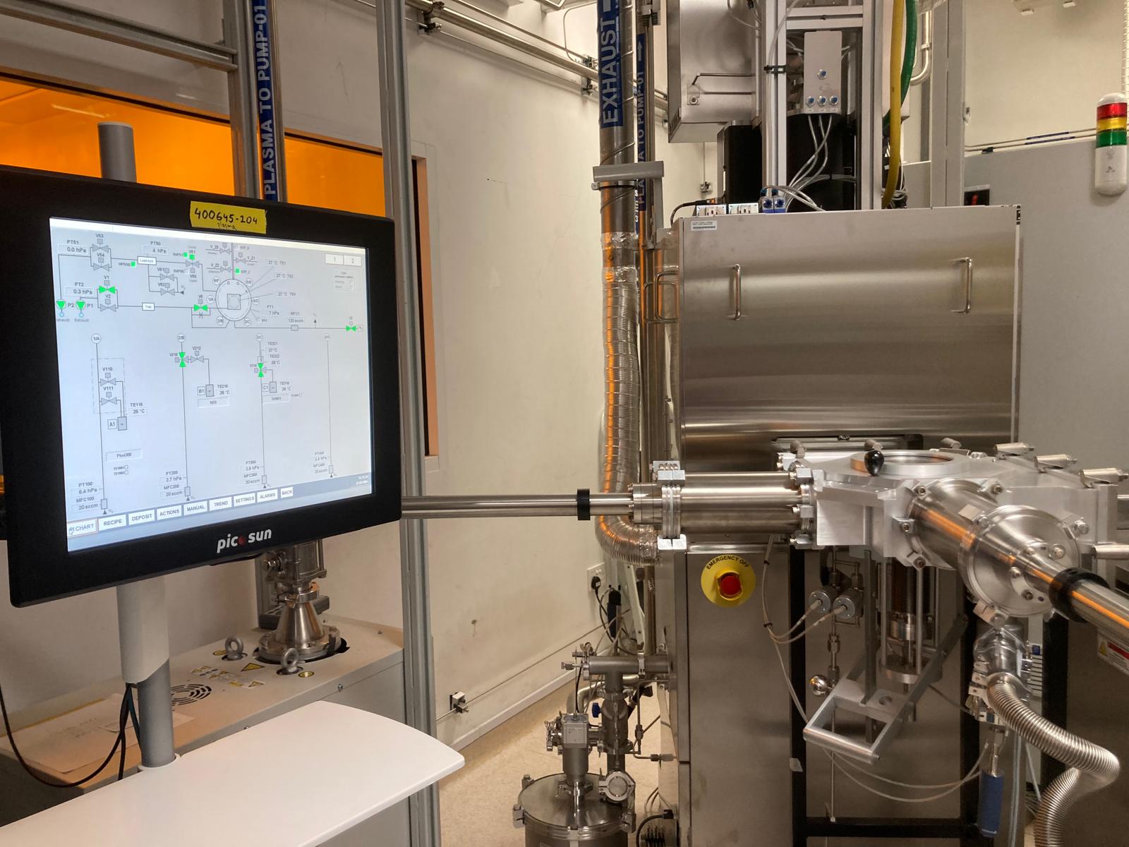
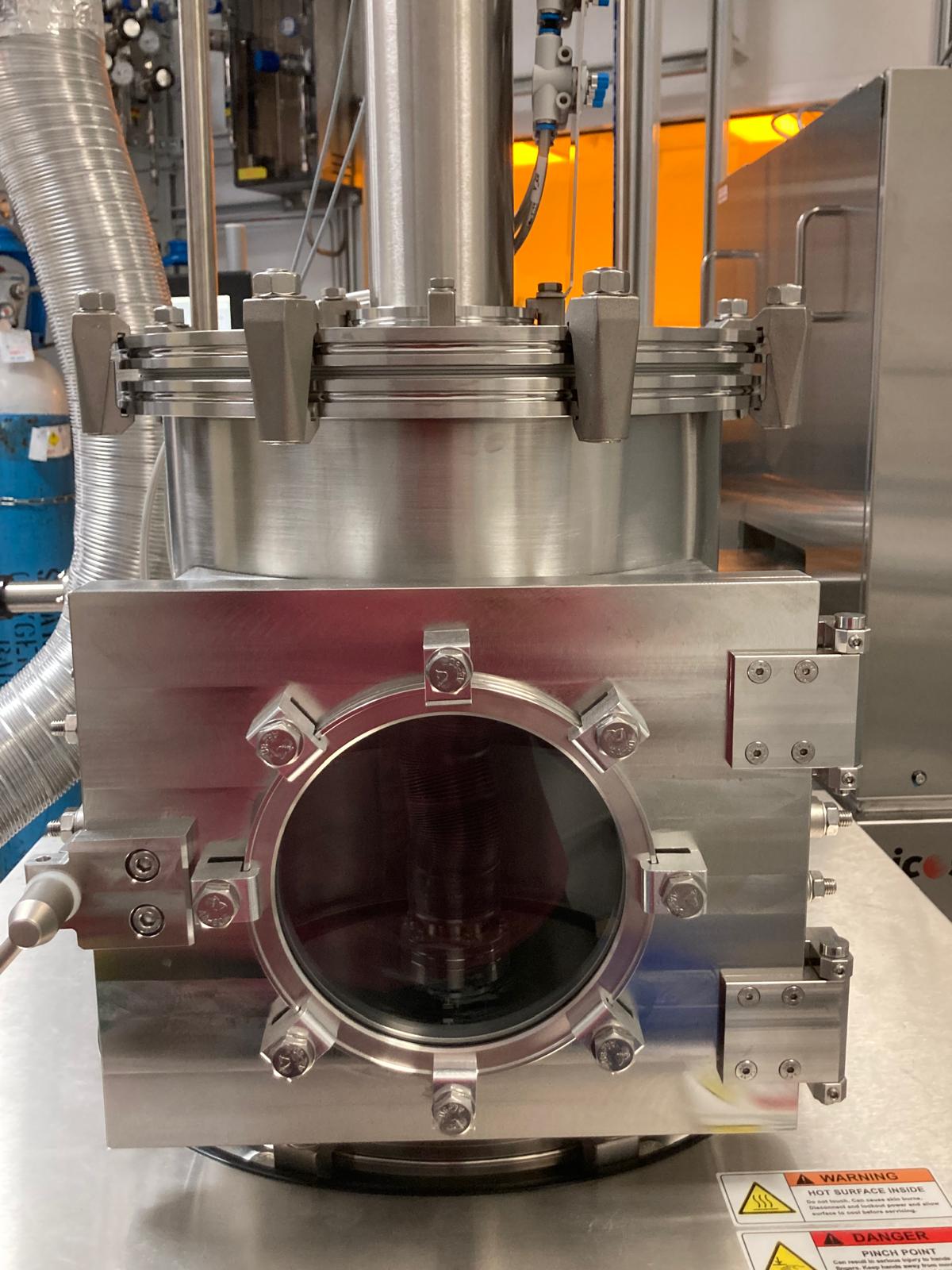
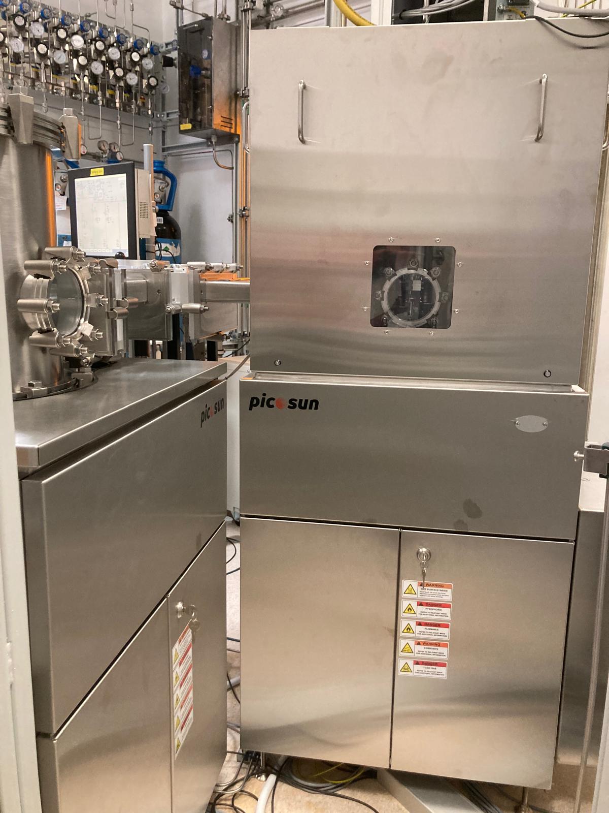
Picosun 200 mm Atomic Layer Deposition Tool
Atomic-scale precision deposition for ultra-thin dielectrics, passivation, and barrier layers with total conformality.
 Lithography
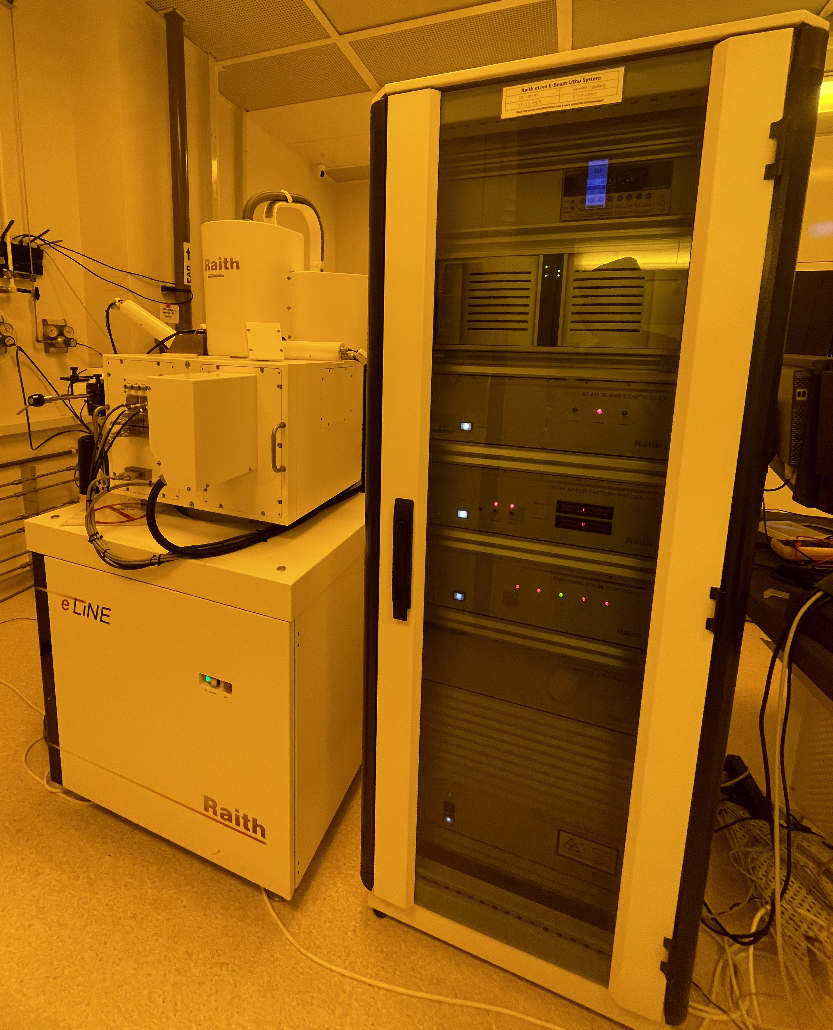
Raith e-Line Electron Beam Lithography
High-resolution pattern generator for ultra-fine nanoscale device patterning and prototype fabrication.
 Lithography
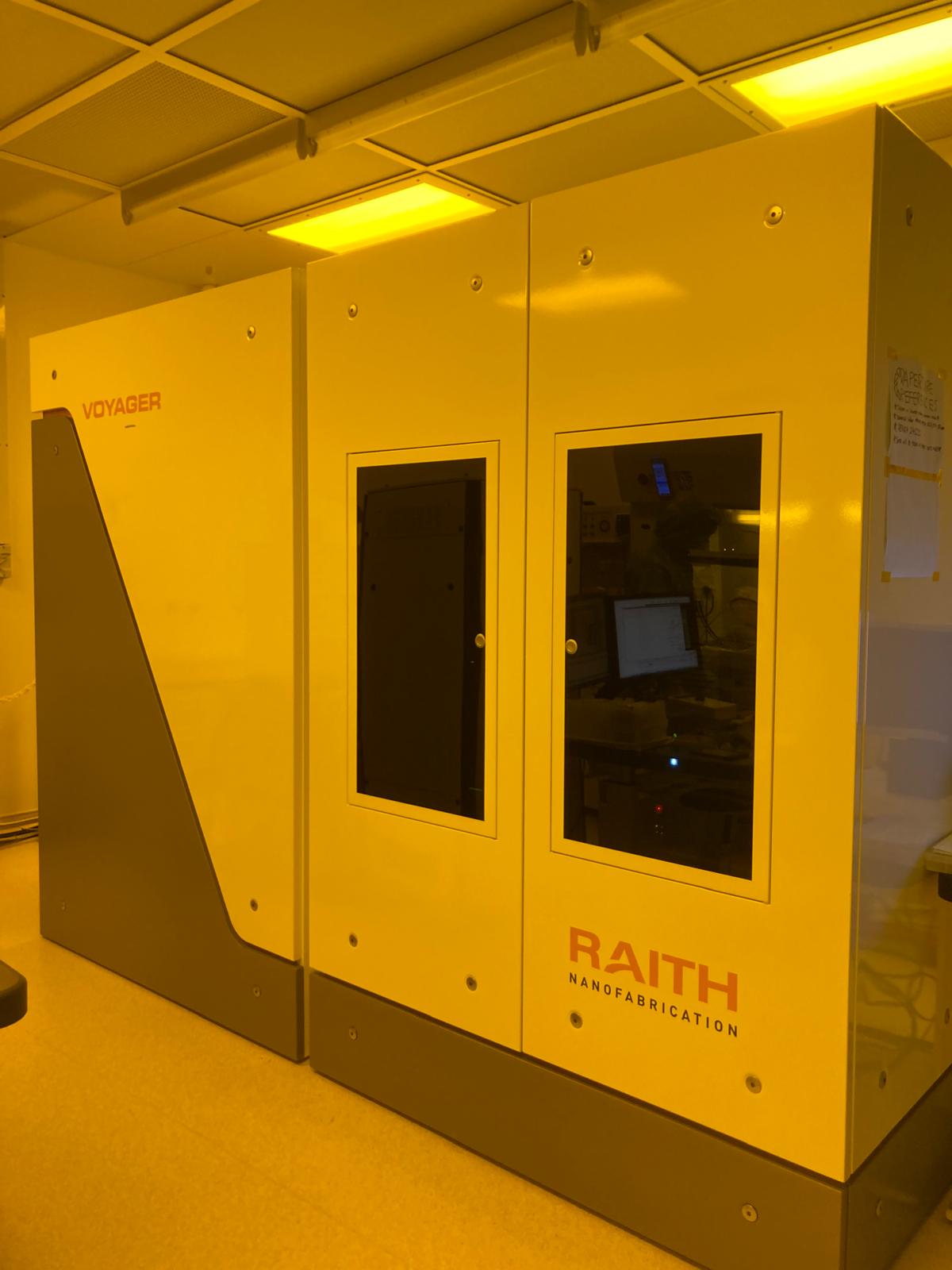
Raith Voyager Electron Beam Lithography
High-speed, scalable e-beam lithography engineered for spintronic devices, photonics, and sub-10 nm structures.
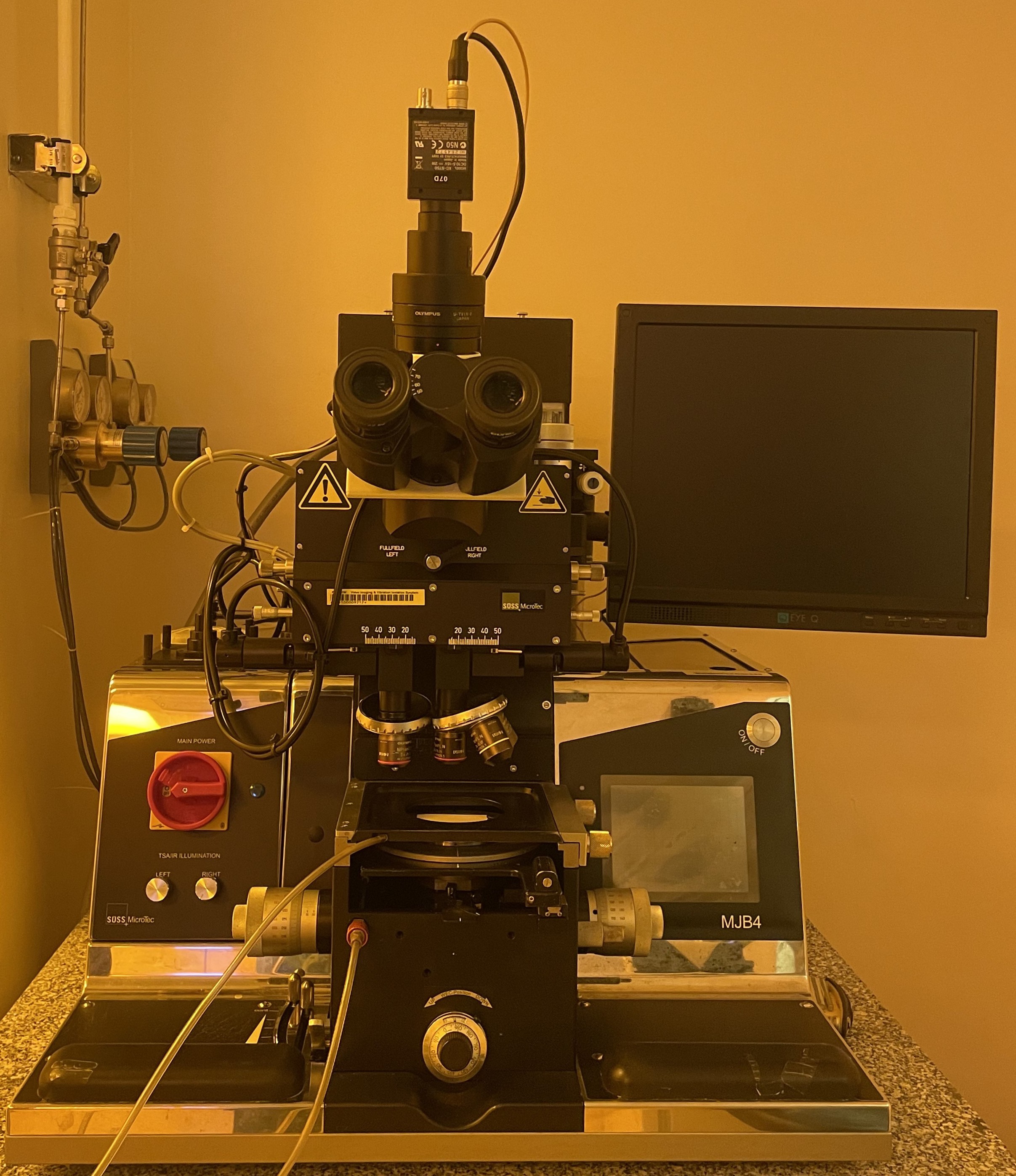 Lithography
Suss Microtec MJB4 Mask Aligner
Precision optical alignment lithography tool for micro-scale contact printing and multi-level mask patterning.
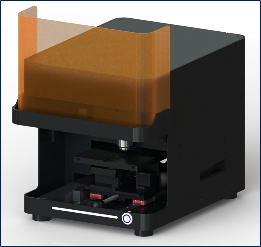 Lithography
Home-developed Patented Desk-Top Maskless Direct UV Laser Lithography System
Small form-factor, desktop, micro-lithography system (800 nm) for rapid prototyping and iterative designs of microfluidic, microelectronic, and MEMS devices for biomedicals, electronics, and sensors, delivering cutting-edge micro-lithography capabilities at a fraction of the cost of competing commercial systems.
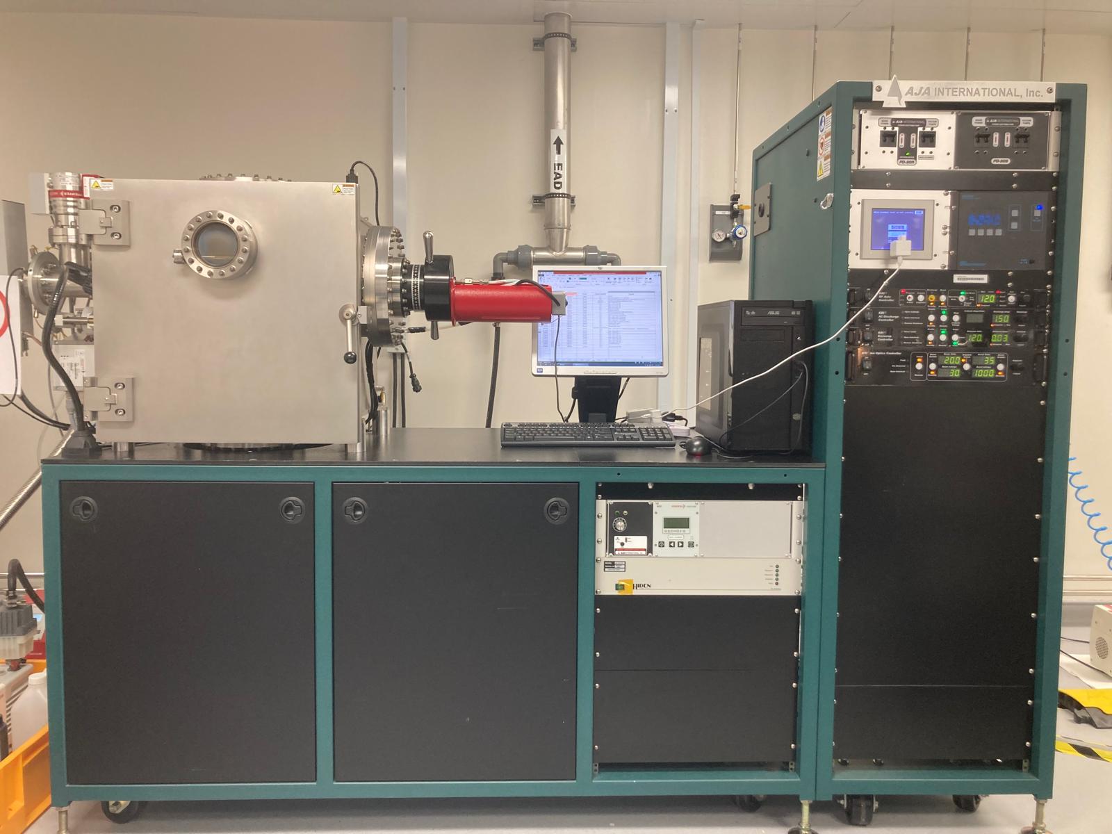 Etching
AJA Ion Milling System with Hiden SIMS Detector
Argon ion beam milling equipped with inline secondary ion mass spectrometry for endpoint detection in magnetic stacks.
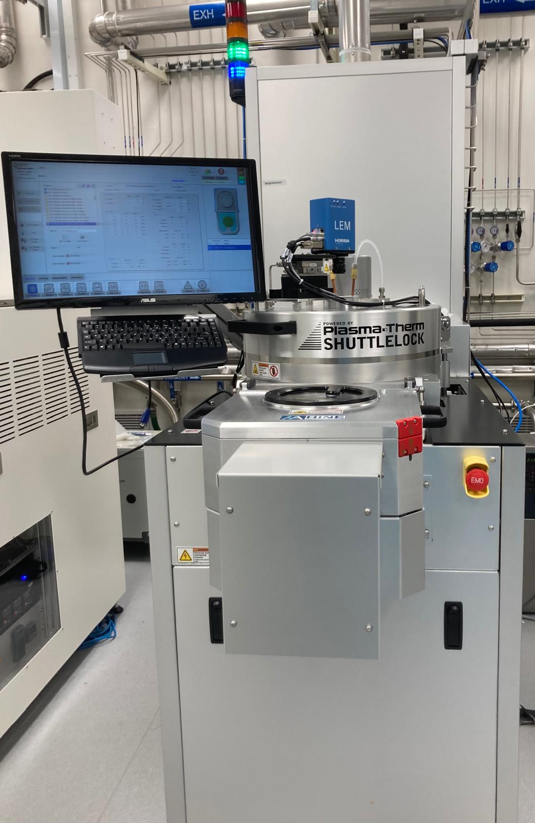 Etch & CVD
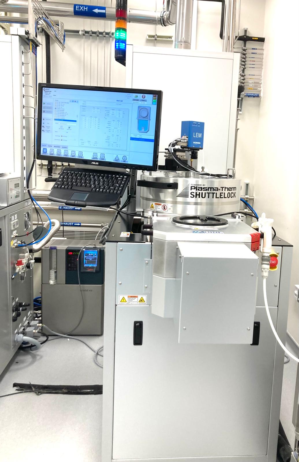
Plasma Therm 200 mm Chamber ICP-RIE System (Fluorine Chamber)
Inductively Coupled Plasma Reactive Ion Etching (ICP-RIE) system specifically for fluorine-based gases.
 Etch & CVD
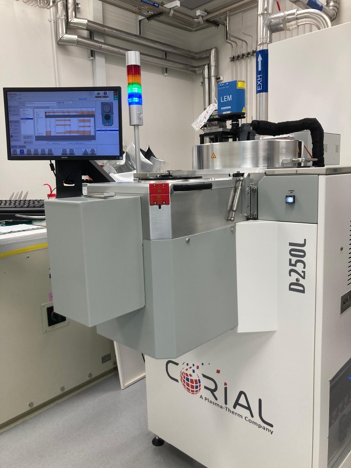
Plasma Therm 200 mm ICP-RIE System (Chlorine Chamber)
Inductively Coupled Plasma Reactive Ion Etching (ICP-RIE) system specifically for chlorine-based gases.
 Etch & CVD
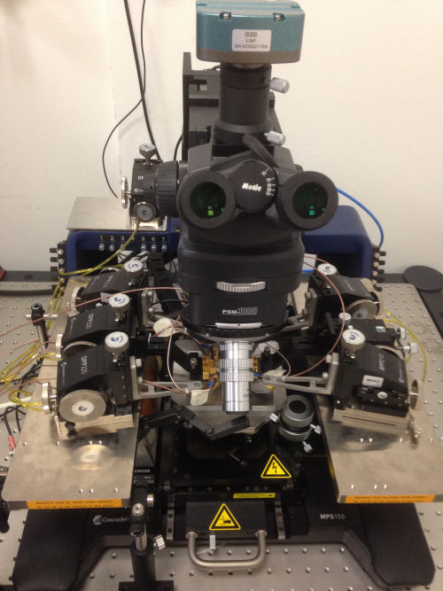
Corial D-250L PECVD System
Designed to deposit uniform, high-quality dielectric layers onto substrates up to 200 mm.
 RF Probing
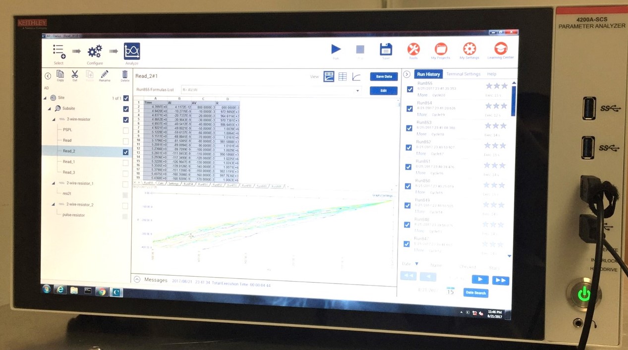
FormFactor (Cascade) Microtech 40GHz RF Probe Station
High-frequency microwave probe station combined with magnetic field application setups for high-speed device dynamics.
 Electrical
Keithley 4200A-SCS Semiconductor Parameter Analyzer
Comprehensive I-V, C-V, and ultra-fast pulsed characterization analyzer for memristive, spintronic, and neuromorphic devices.
 Electrical
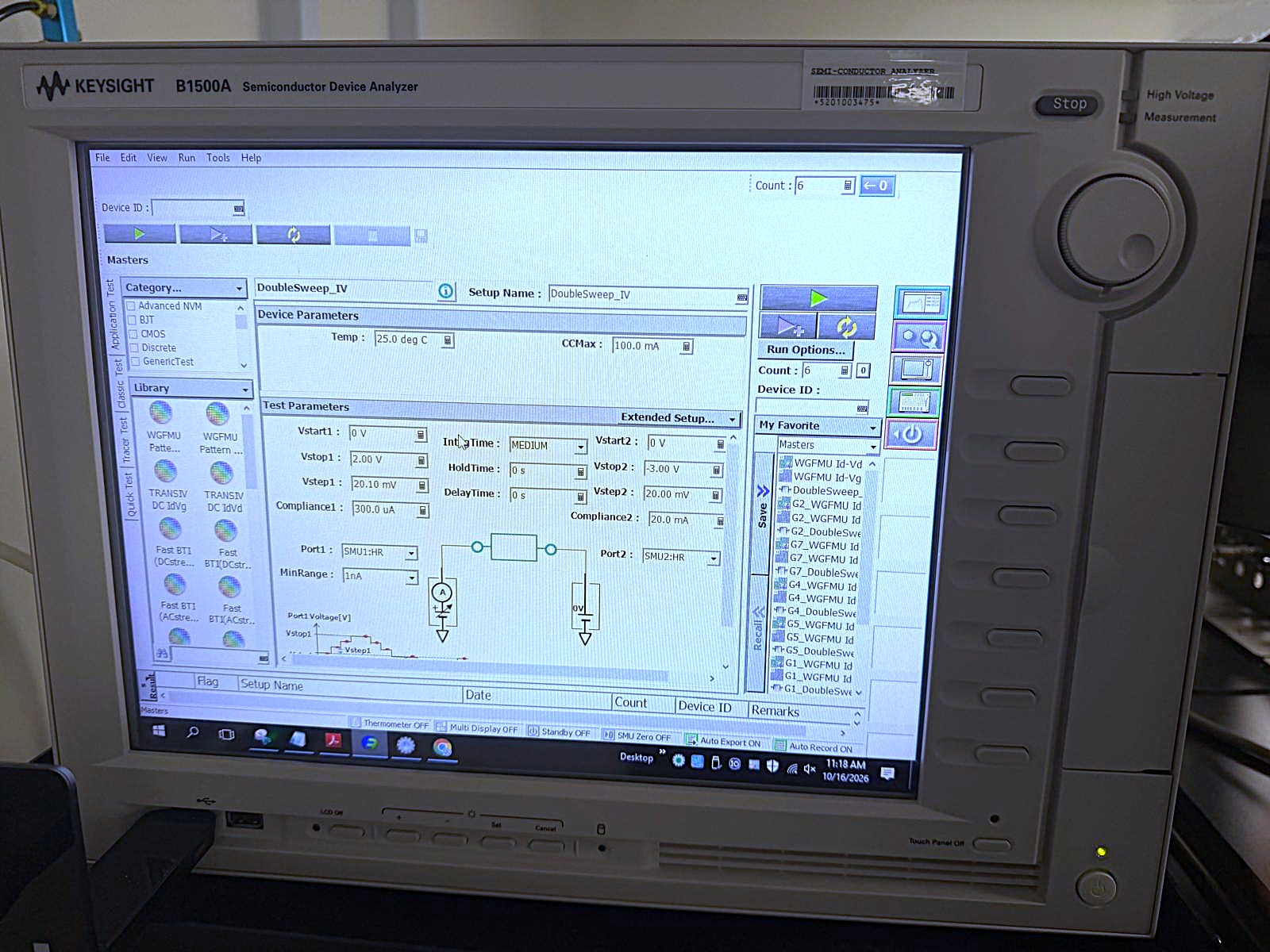
Keysight B1500A Semiconductor Device Parameter Analyzer
Comprehensive I-V, C-V, and ultra-fast pulsed characterization analyzer for memristive, spintronic, and neuromorphic devices.
 Microscopy
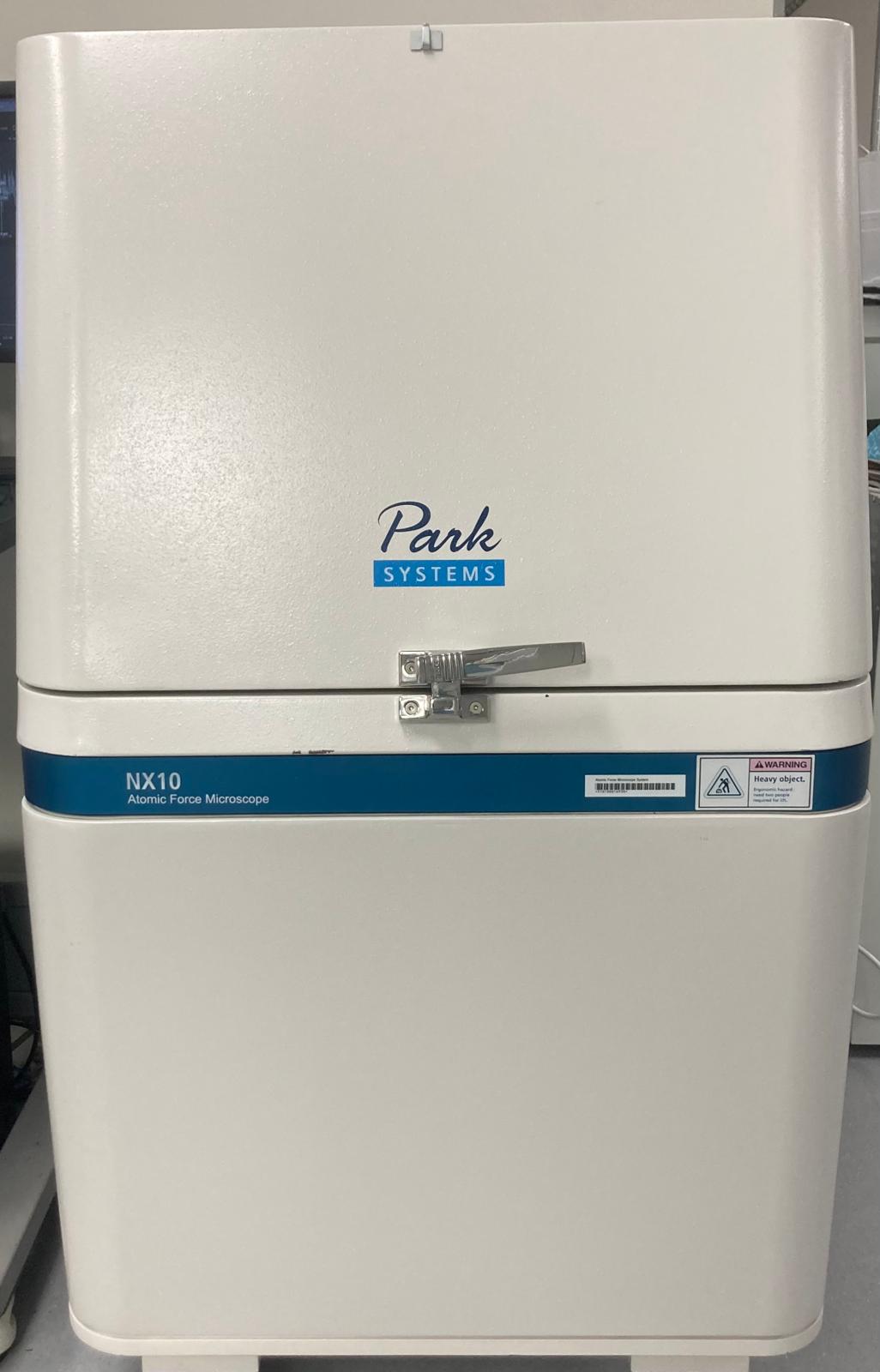
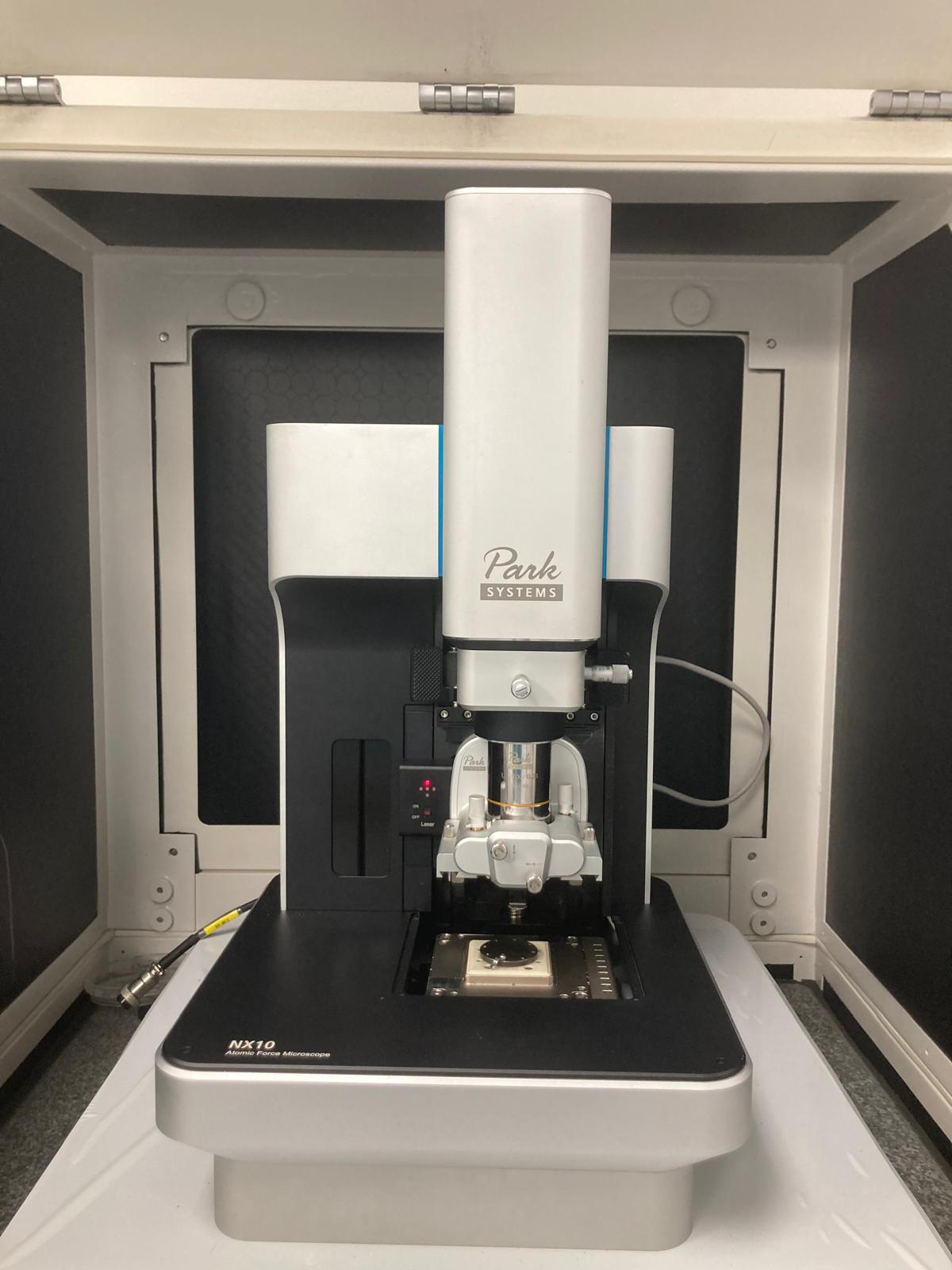
Park Systems NX10 Atomic Force Microscope
AFM optimized for small-sample nanoscale research and recognized for combining high-accuracy topography data.
 Polishing
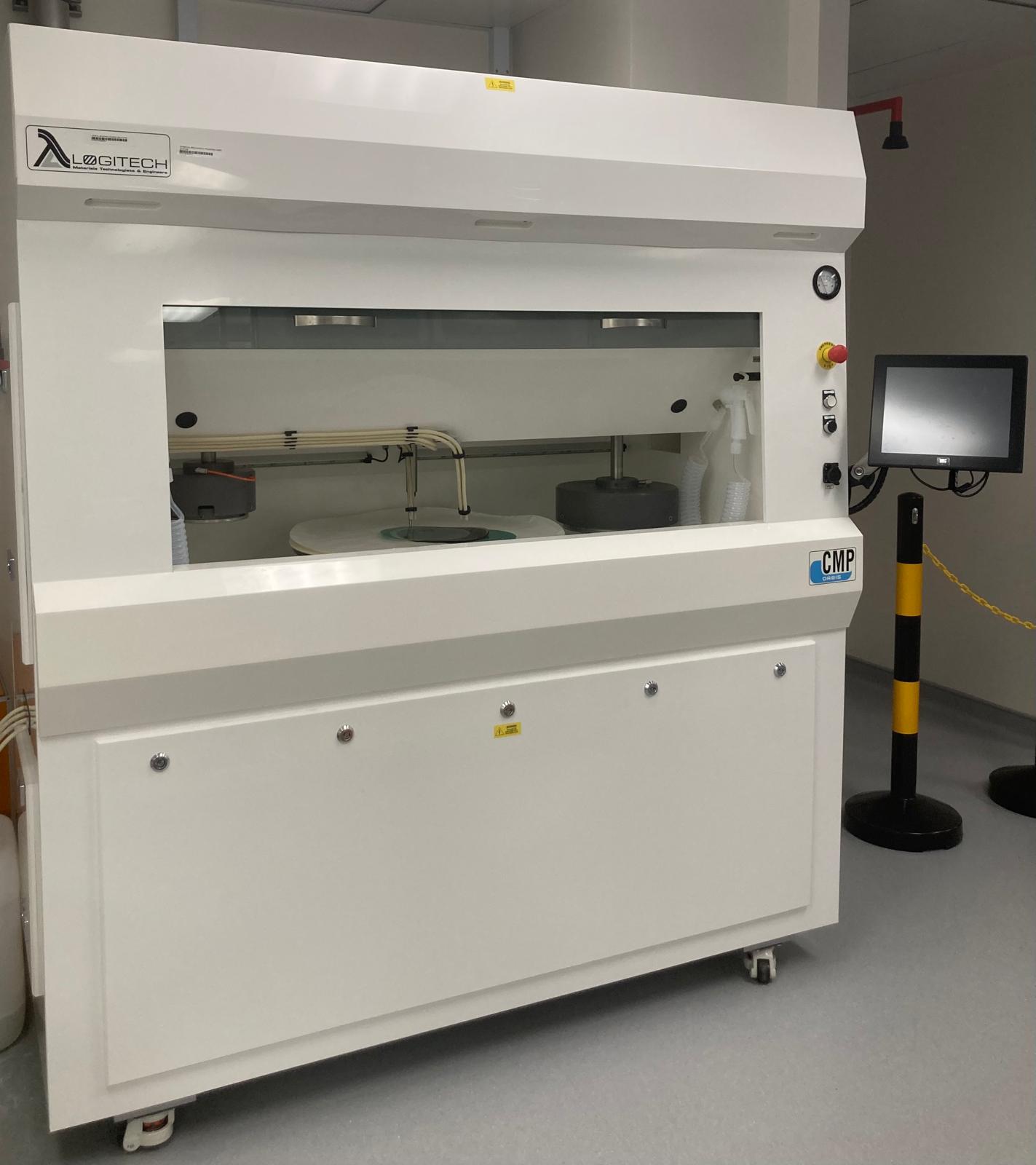
Logitech CMP Orbis system
Engineered to facilitate IC manufacturing, MEMS, Opto-MEMS, and Bio-MEMS fabrication while supporting development environments requiring production-level accuracy.
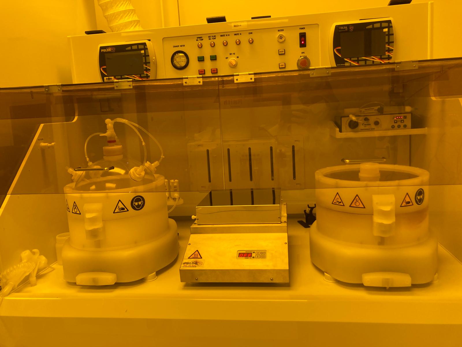 Spin Coat
ing Station
Deposits uniform thin films onto flat substrates, such as silicon wafers, glass plates, or optical lenses.
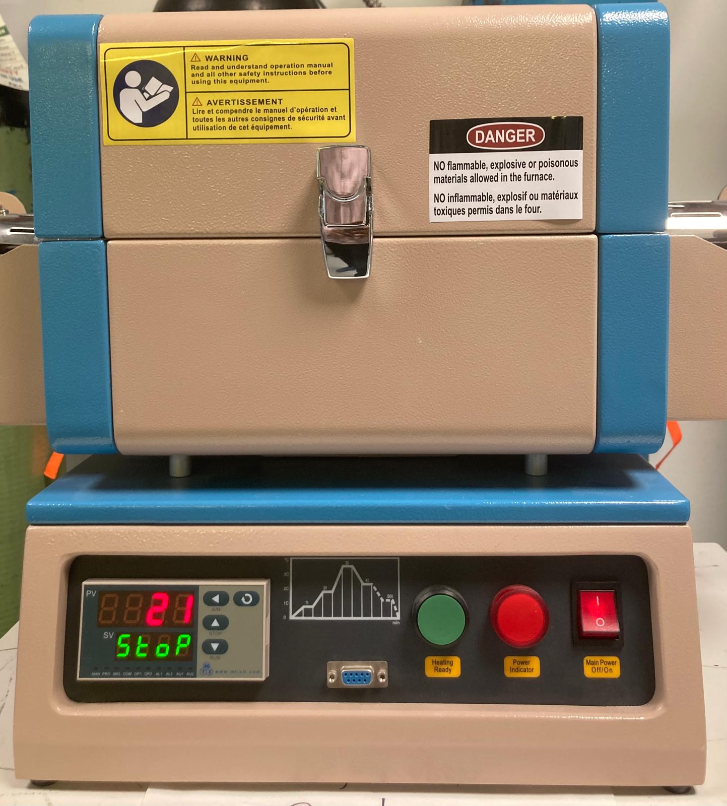 Annealing
MTI's Compact Split Tube Furnace
Thermal processor for calcination, sintering, chemical vapor deposition (CVD), and annealing.
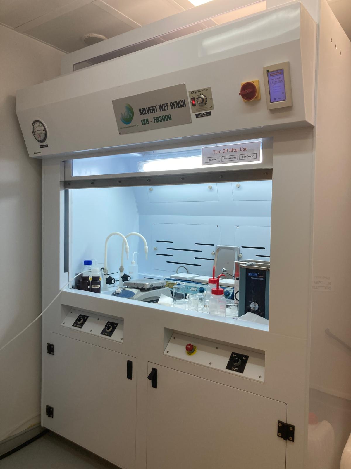 Wet Processing
Solvent Wet Bench
Engineered for microfabrication and semiconductor processing.
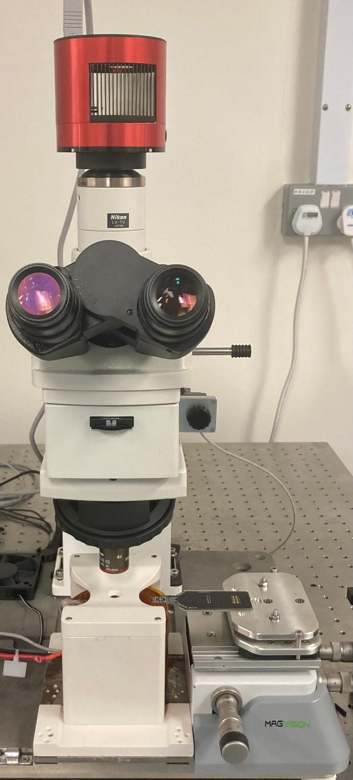 Microscopy
Kerr Microscope
Customized to visualize magnetic domains and magnetization dynamics at the nanoscale.
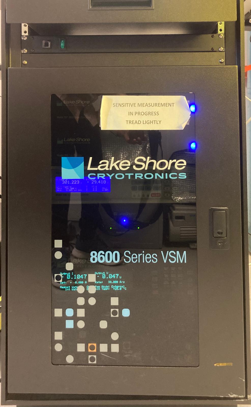 Magnetic Characterisation
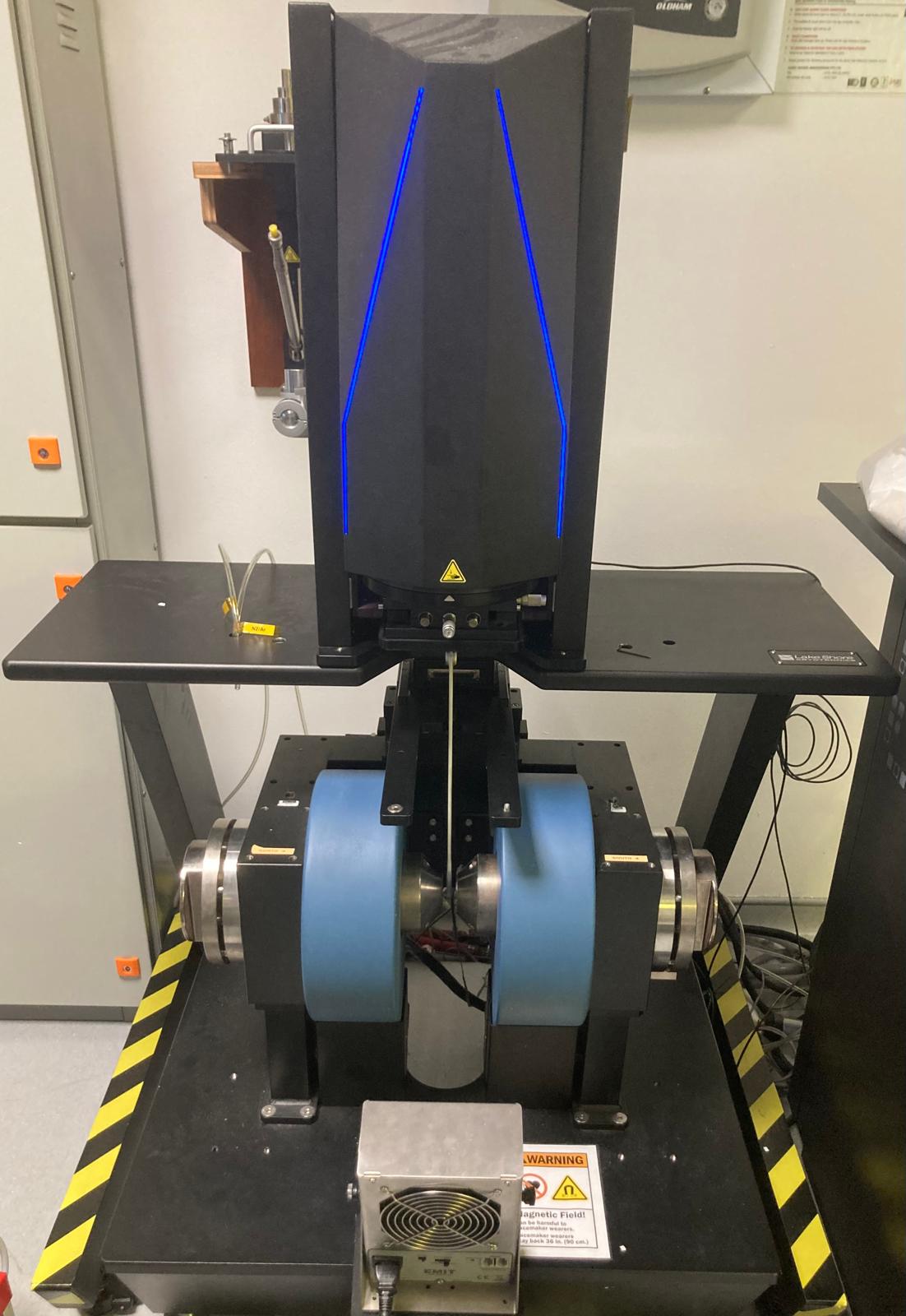
Lake Shore Cryotronics 8600 Series Vibrating Sample Magnetometer (VSM)
To characterize the magnetic properties of solid, liquid, powder, or thin-film samples.
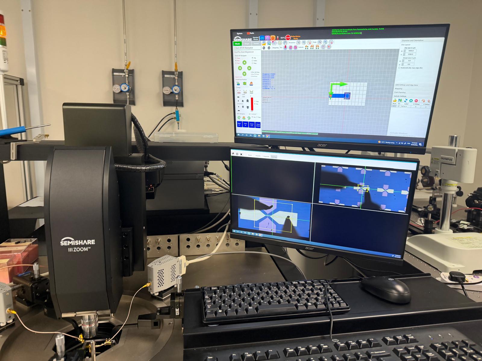 RF Probing
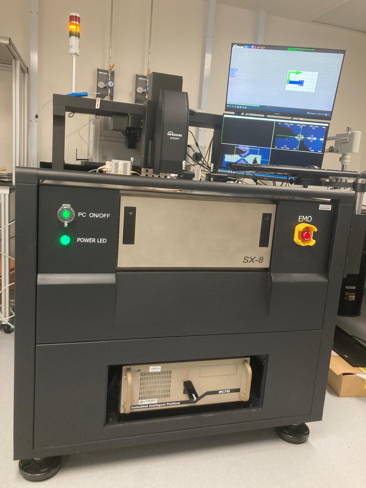
SEMISHARE SX-8 Semi-Automatic Wafer Probe Station
Highly efficient semi-automatic wafer probe platform specialized in testing the performance of various advanced chips.
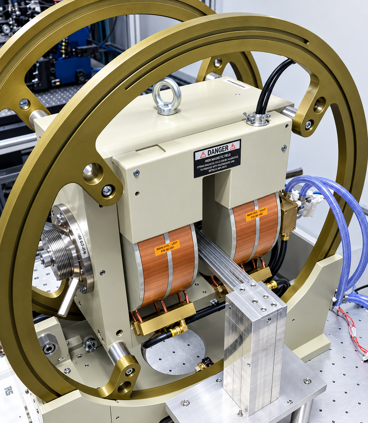 Magnetic characterisation
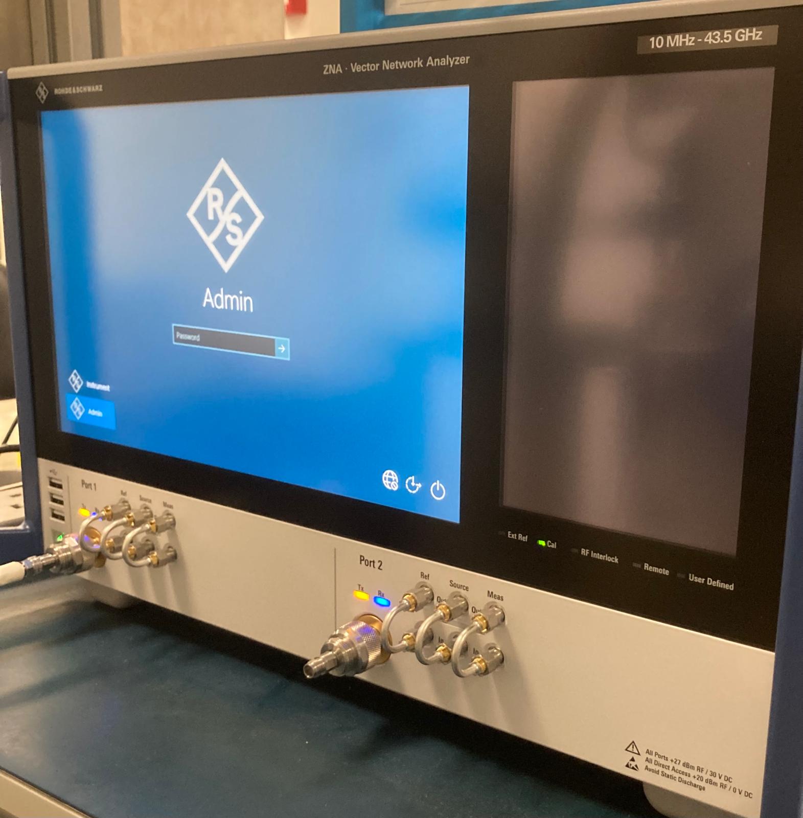
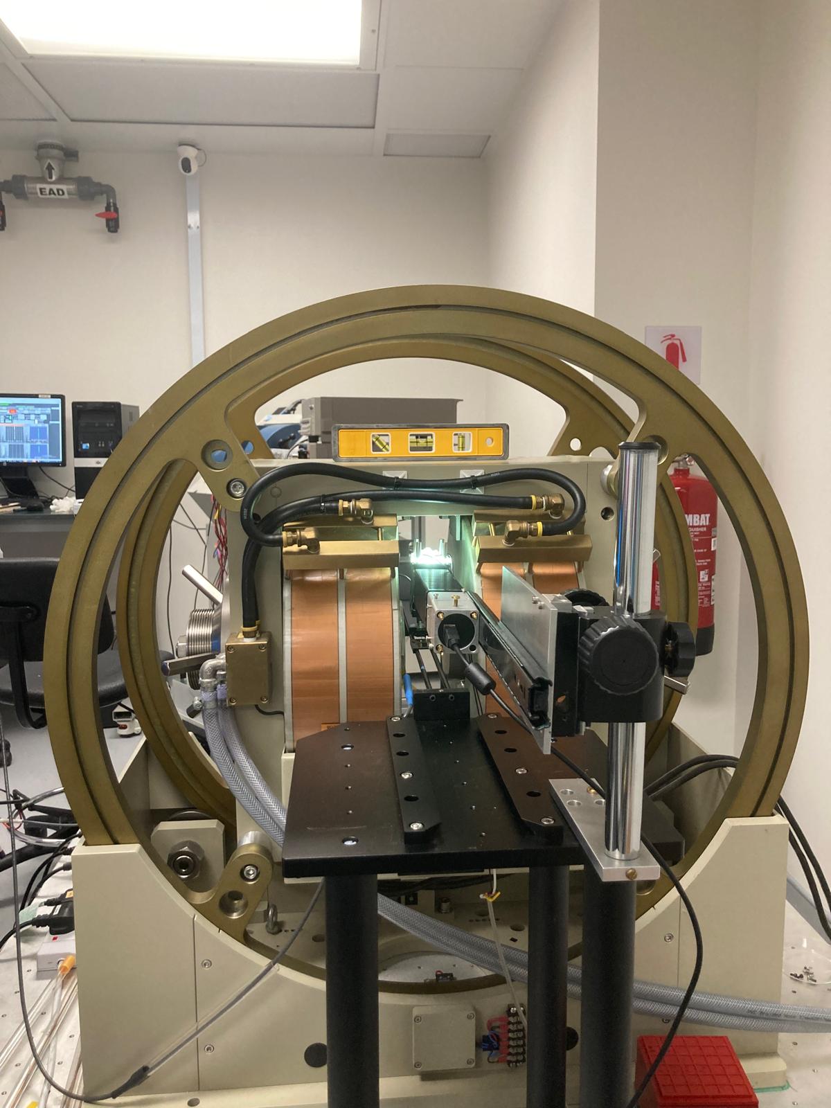
VNA-based Ferromagnetic Resonance Spectrometer
Customized to measure and analyze current-induced magnetization dynamics in nanoscopic magnetic systems and thin-film heterostructures.
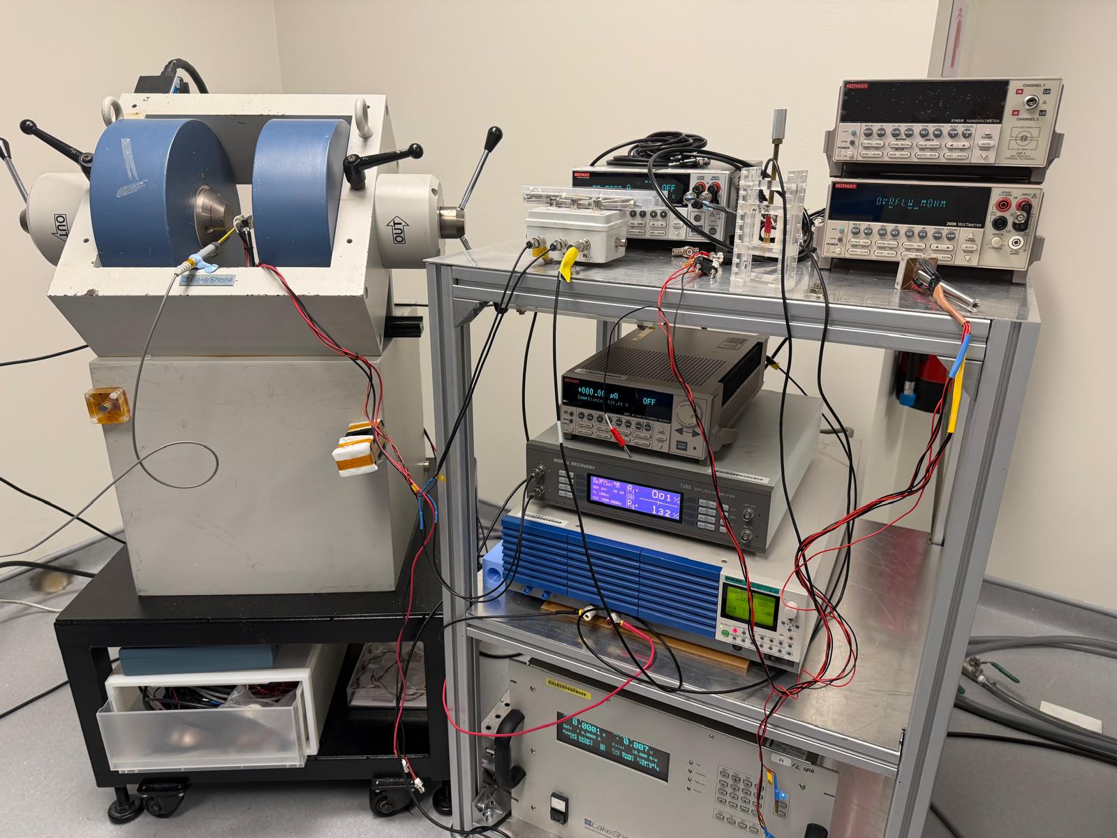 Magnetic Characterisation
Spin Transport Measurement System
Customized to measure and analyze current-induced magnetization dynamics in nanoscopic magnetic systems and thin-film heterostructures.
 Central
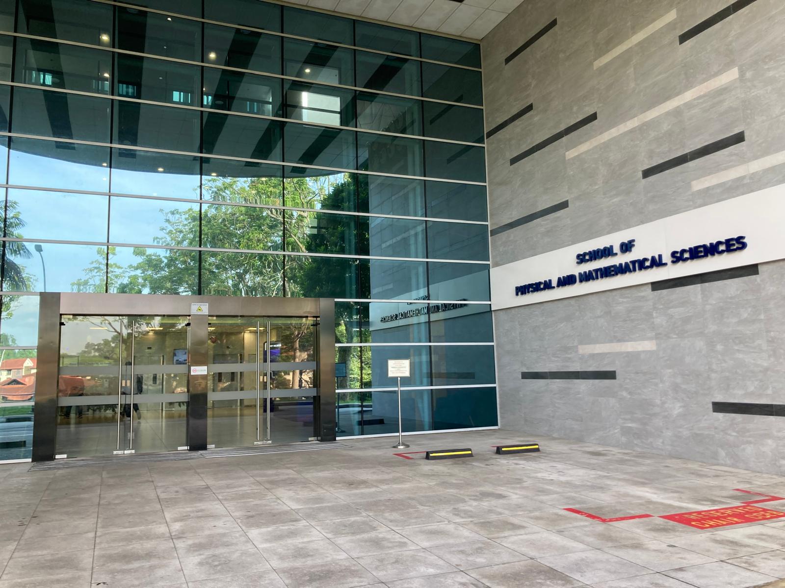
School of Physical and Mathematical Sciences | Division of Physics and Applied Physics | Central Facilities & Services
Explore additional departmental shared facilities and support services available for research and testing.
No matching equipment found
Try searching for a different keyword or choosing another category.